DMA basics on the UltraMyir board
The UltraMyir is an FPGA development board by MYIR tech based on the Zynq Ultrascale+ ZCU3EG with plenty of interesting peripherals like FMC, PCIe, SATA, QSFP, that will surely fullfil the needs of many projects.
DMA (Direct Access Memory) is a peripheral, also found in processors, that automates moving data from one memory location to another. In case of Xilinx FPGA it is typically used to stream data from memory to a processing block. All that happens without software intervention, except for the start.
Xilinx FPGA cores use AXI (Advanced Extensible Interface) for data transfer. AXI4 is the current revision. AXI comes in two main flavours: memory mapped (where each byte of word has an address to be in) and stream (where data is continuous like in video). They are called AXI4 and AXI4-Stream, respectively. There is also AXI4-Lite, a lightweight variant of memory mapped AXI4.
Large pieces of data will typically sit on external RAM, for example the DDR RAM attached to the PS (Processor System). It is possible to access RAM data from the PL using the PL-PS interfaces and DMA blocks as shown in this example design. The DMA block will run concurrently with the PS so the software can run other tasks and even access the RAM (apparently) simultaneously.
In this example, the AXI4 DMA is used to fetch a block of data from RAM, stream it to itself and put it back into another RAM area. It may look like not much useful but it is the base for hardware acceleration, just by inserting a processing block in the data stream as we will see in future projects.
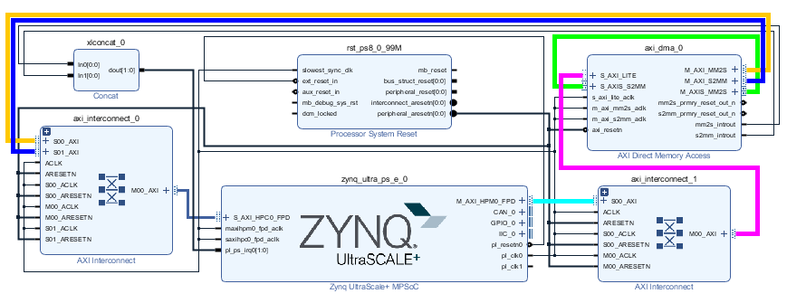
The project TCL and files are available on github. If you are confident enough, just download them, build the project, test it and adapt it to your needs. The rest of this article is a pedagogic introduction. Below is the block diagram of the project.

The main blocks are the Zynq processing system, the AXI interconnects and the DMA. The concat and processor reset are for bringing interrupts into the PS and managing the reset of peripherals.
AXI busses are highlighted in color to follow them easily. Rest of nets are clock (from the PS), reset and interrupts.
The DMA is configured as shown below. Scatter gather mode is disabled and both Read and Write modes enabled. "Read" means from memory mapped to stream (MM2S) and "Write" is the opposite data direction (S2MM).

The address width must match the Zynq PS that is 40 bit. The memory mapped data width is set to 32 bit to match the ports in the PS, although they could be different. The M_AXIS_MM2S is connected to S_AXIS_S2MM, so the data streamed goes straight back to memory. Here is where processing blocks can be attached to receive serialized data and return the result.
Finally, the two interrupts in the DMA are concatenated and fed into the PS. They will be triggered when a transfer is finished so the software only needs to start the read and write processes.
The software is based on the SDK example xaxi_dma_example_simple_intr. I only added the function XTime_GetTime to measure the transfer time, as shown below.

See this and more projects with the UltraMyir board at:
Electrical Engineer at Petrobras
4yVery useful article to get some insights into Zynq devices.